
Digital Blocks offers the DB9000 family of programmable Display Controller Verilog IP Cores for systems requiring TFT LCD or OLED panels in their product. The DB9000 TFT LCD / OLED Controller IP Cores are offered with a customer-specific range of features, supporting basic display applications up to optional advanced features.
Display Controller IP
Digital Blocks Display Controller Verilog IP Cores target ASIC/FPGAs design teams with system applications in Medical, Industrial, Aerospace/Defense, Automotive, Computer, Monitor, Consumer, AR/VR Headsets, IoT, Wearables, Signage, Gaming, Broadcasting, & Test Instrumentation. Digital Blocks offers releases containing a variety of optional features from basic baseline display requirements up to advanced display processing features.
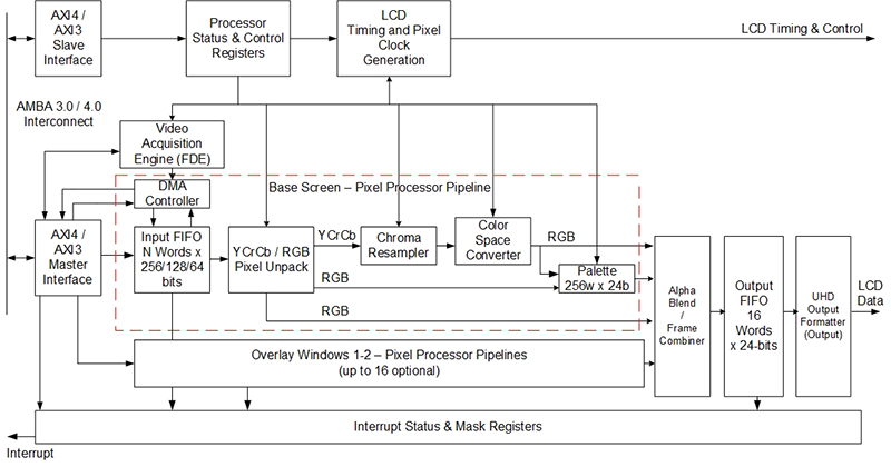
Advanced Display Controller IP Block Diagram (Example Configuration)
Configuration Options
Every DB9000 shipment is a synthesizable Verilog RTL core, not a fixed netlist. Bus
protocol, bus width, memory technology, and FIFO sizing are all set by
`define / parameter before synthesis, and each advanced feature below is
only built into the gate count if you license and enable it — so an unlicensed feature
costs zero silicon.
Core Synthesis Parameters
Available in every DB9000 configuration, no licensing required.
- Bus Protocol & Interconnect: AMBA AXI4, AXI3, AHB, AHB-Lite, AHB5, APB, or Altera Avalon-MM — selected by a single
`define. - Master Bus Data Width: 32-, 64-, 128-, 256- or 512-bit master bus, sized to the target resolution and bandwidth.
- Memory Technology Target: Palette, FIFO, and Cursor memories instantiate through one wrapper module, pre-built for Xilinx, Altera, Actel, or a generic vendor RAM — or substitute your own.
- Synchronous / Asynchronous FIFOs: Input/Output FIFOs default to synchronous; a single define switches to asynchronous, unregistered-output memories.
- Configurable FIFO Depth: Input FIFO address width sets FIFO depth — typically 16 words for small panels, up to 2K words for large, high-resolution panels, with data width scaling to the master bus.
- Pixel Clock Source Select: Internal clock-mux architecture with full CR1 programming, or a direct bypass define that drives the pixel clock straight from
PCLK_IN. - Register Bit Trimming: Any unused Control & Status Register bit can be removed and hardwired as a parameter instead — typically halving VLSI footprint versus a fully-populated register set.
- DFT Test Bus Passthrough: Optional per-memory DFT test buses netlist up to the top level for scan/BIST insertion.
Licensing & Synthesis Options
Optional RTL add-ons, each independently licensable and synthesized only when enabled.
Multi-Window Compositing
Overlay Windows
1, 2, 4, 8, or 16 independently positioned, DMA-fed overlay windows composited over the base screen, each with its own enable, X/Y start-end, and frame-buffer address registers.
Alpha Blend
Per-pixel alpha compositing of an Overlay Window over the base screen at 16/18/24 bpp, with an 8-bit alpha channel and programmable alpha inversion.
Hardware Cursor
32×32 or 64×64 pixel hardware cursor with its own palette, X/Y positioning, and clip registers, sourced from a dedicated dual-port cursor buffer memory — zero host involvement per frame.
Image ScalarPreliminary
In-line image scalar within the display controller IP for ASICs — scaling is applied directly to the pixel stream before it reaches the display interface, with independent scaling per plane.
Color Space & Chroma Processing
Chroma Resampler — 4:2:2 / 4:2:0
Up-samples packed YCbCr 4:2:2 (2-tap FIR) or planar 4:2:0 video (parallel-DMA, cubic-convolution engine) to 4:4:4 ahead of color-space conversion.
Color Space Conversion
Programmable 4×4 matrix (10-bit signed coefficients, 8-bit summands) converts YCbCr to gamma-corrected RGB, with selectable truncate/round and saturate/clamp behavior; up to three instances — base screen plus two overlay windows.
High Dynamic Range (HDR)Preliminary
HDR10 / HLG pixel path: 30 bpp (10:10:10) frame buffers, 10-bit output dithered to 8-bit panels, programmable PQ / HLG / BT.1886 LUTs, a BT.709 ↔ DCI-P3 ↔ BT.2020 gamut matrix in linear light, and BT.2390 tone mapping. ST 2086 metadata sideband. Optional 3D LUT and per-plane HDR.
Advanced Panel Interfaces
LVDS Serializer (OpenLDI)
OpenLDI V0.95-compliant serializer driven by a customer-supplied 7× pixel clock, generating 18- or 24-bit RGB LVDS output pairs plus VSYNC/HSYNC/DE — Unbalanced mode standard, Balanced mode by request.
Multi-Port / Multi-Link Interface + UHD Output Formatter
1, 2, 4, or 8-lane output to DisplayPort, HDMI, V-by-One, MIPI, or LVDS panels, with single/dual/quadrant screen-area partitioning for UHD/8K displays. Supersedes the earlier fixed 2-port interface as of Release 1.15.0.
Dual Display Support
Splits one unified frame buffer line in half in hardware to drive independent left/right displays from a single pixel pipeline running at 2× pixel clock.
Dynamic Content Engine
Frame Descriptor Engine
Linked-list DMA engine that reprograms the base-screen and up to 16 overlay-window frame-buffer addresses before every frame with zero host CPU intervention — built for streaming video playout.
Diagnostics & Reliability
Test Pattern GenerationPreliminary
On-demand RGB color bars, grayscale gradient, or border-grid test patterns triggered by a register write — no external stimulus required.
CRC Check Per RegionPreliminary
Hardware CRC-802.3 checking of incoming frame-buffer pixel data across 32-, 64-, 128-, 256- or 512-bit AXI widths, with programmable per-region checking and automatic retransmission or interrupt on error.
Frozen Display MonitorPreliminary
Watchdog-timed monitor of VSYNC/HSYNC/DE and the DMA base-to-current-address heartbeat, with optional automatic self-reset and re-run on a detected fault.
Full register-level detail for every option above is documented in the DB9000 Technical Reference Manual. Contact Digital Blocks to discuss licensing, window/lane counts beyond the standard configurations, or a synthesis configuration not listed here.
Interface & Bus Variants
The DB9000 TFT LCD / OLED Display Controller ships in interconnect-matched variants — pick the bus fabric your SoC or FPGA design already uses.
DB9000AXI4 / DB9000AXI3
AMBA AXI4 & AXI3 — primary variant
- Bus Width: 512, 256, 128, 64, or 32-bit AXI4 interface to frame buffer memory. DB9000AXI3 is a slight subset, supporting the AXI3 interconnect in place of AXI4.
- Panel Ports: Programmable 1, 2, 4, or 8-port LCD/OLED panel interface.
- Display Interfaces: Optional LVDS link layer, plus MIPI DSI, DisplayPort, DVI, HDMI, or V-by-One transmitter interfaces.
- Resolution Range: 8K/4K high-resolution displays down to 320×240 panels.
- AXI4 Compliance: Burst lengths greater than 16 beats per memory request, plus Quality of Service (QoS).
- Deliverables: Simulation test suite, Linux driver, Synopsys Design Constraints (SDC), and user manual.
DB9000AXI5
AMBA AXI5 & ACE5-Lite — coherent, real-time, safety-ready
- I/O Coherency: ACE5-Lite ReadOnce reads frame buffers straight from CPU and GPU caches — no software cache maintenance.
- Bandwidth & Latency: MPAM partition IDs and per-requester QoS allocate a fixed share of memory bandwidth; chunking cuts time-to-first-pixel.
- Functional Safety: AXI5 check/parity signals plus data-poison detection with a programmable safe-state response.
- Protected Media: NSAID and RME identifiers read TrustZone-protected HDR and DRM surfaces the host CPU cannot.
- Property-Selectable: Each AXI5 feature is an independent synthesis option; all disabled equals DB9000AXI4.
- Deliverables: Simulation test suite, Linux driver, Synopsys Design Constraints (SDC), and user manual.
DB9000AHB / DB9000AHB-Lite / DB9000AHB5
AMBA AHB family — silicon-verified
- Interfaces frame buffer memory and an ARM processor via the AMBA AHB bus fabric to TFT LCD panels.
- AHB-Lite Variant: DB9000AHB-Lite offers an AHB-Lite Master interface, typically for a point-to-point connection to a multi-port memory controller.
- AHB5 Variant: DB9000AHB5 targets the newer AMBA 5 AHB bus fabric.
- Deliverables: Comprehensive test suite, synthesis scripts, datasheet, and user manual.
DB9000AHB Datasheet (PDF) | DB9000AHB-Lite Datasheet (PDF) | DB9000AHB5 Datasheet (PDF)
DB9000AVLN
Altera Avalon Bus — Verilog & VHDL
- Interfaces frame buffer memory and an Altera NIOS II or ARM processor via the Altera Avalon Bus to TFT LCD panels.
- Deliverables: Comprehensive test suite, software driver, synthesis scripts, datasheet, and user manual — available in both Verilog and VHDL.